|
| ||||||||||||||||||||||||||||||||||||||||||||||
|
Section: Science Life |
deutsche Version  Print-Version |
|
FIRST Lab with a new coating technique Ultrathin layers | |
|
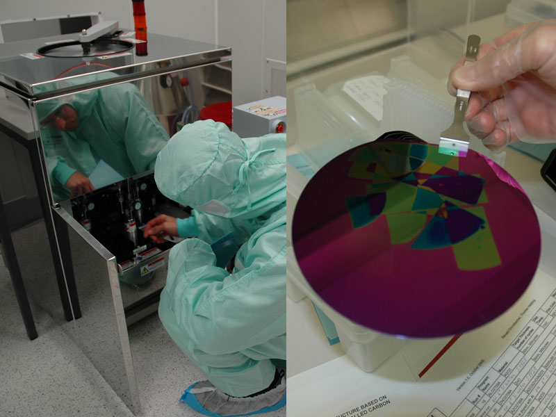
“Atomic Layer Deposition” (ALD) is the name of a technique that enables the preparation of very thin homogeneous layers of uniform thickness. ETH Zurich uses ALD layers for example to develop miniaturised pressure sensors and for general research in the nano region. By Beatrice Huber The equipment stands as clean as a whistle in the FIRST Lab and enables ETH Zurich to carry out what is known as “Atomic Layer Deposition” (ALD). "ALD allows ultrathin, extremely uniform layers to be applied to surfaces with geometries of any kind,” is how Ronald Grundbacher explains the advantages of ALD. Grundbacher carries out research as a scientist in Professor Christofer Hierold’s group(1) and looks after the ALD machine for the FIRST Lab. The ALD technique was invented more than 30 years ago by the Finnish scientist Tuomo Suntola – the machine at ETH, a SUNALE R-150 made by the Picosun Oy Company, also comes from Finland – and has recently come into greater use in the semiconductor industry. According to Grundbacher, the reason for this is probably that advances in the miniaturisation of chips, sensors and memory elements necessitate ever thinner, conformal and defect-free coatings. These are exactly the coatings that ALD provides. The equipment in the FIRST Lab is one of the first of its kind in Switzerland and can apply aluminium oxide and zinc oxide to wafers with a maximum diameter of 150 millimetres. Insulators, semiconductors, metals ALD builds up layers chemically on a substrate surface. Using two different source materials (A and B), two half-reactions take place between the substrate surface and the source materials at a reaction temperature between 150 and 450°C. This involves introducing A and B alternately into the reaction chamber, and complete reaction takes place on the substrate surface. The chamber is purged with nitrogen each time between the two source materials, thus achieving complete separation between A and B. ALD generates layers on flat surfaces such as on a wafer, but can also do so on other geometries. There have been experiments with three-dimensional MEMS (Micro-Electro-Mechanical System) structures and even with PET (polyethyleneterephthalate) bottles.
|
ALD enables various materials to be applied, including insulators, semiconductors or metals, or even wear-resistant or corrosion-resistant coatings. In the electronic components area ALD is attractive for good dielectrics (gate oxide, capacitor dielectric) or diffusion barriers for copper. In the mechanical engineering field the thin, uniform layers display interesting properties for micro- and nano-mechanisms. Miniature pressure sensors Professor Hierold’s research group at ETH Zurich is using ALD to develop a miniature pressure sensor. Doctoral student Thomas Helbling developed the pressure sensor, which consists of an ultra-thin aluminium oxide membrane onto which carbon nanotubes are anchored. These nanotubes are the actual sensor elements.(2) During the preparation an ALD layer of aluminium oxide, which will afterwards be the sensor membrane, is applied to a silicon wafer. As source materials the ETH researchers use trimethylaluminium for the first half-reaction and water for the second half-reaction, and they allow the layer to grow to about 100 nanometres in several hundred cycles. Previously this process step was carried out by partners in the USA, and although very successful, it was also inconvenient for the researchers. The ETH researchers have now been able to do this in the FIRST Lab for just over a month. Grundbacher says this is a great relief that gives greater flexibility for further optimisation of the ALD layers, the pressure sensors and in nanotechnology research. Micro-Electro-Mechanical System, MEMS The pressure sensor that has been developed is known as a Micro-Electro-Mechanical System, abbreviated MEMS. This system is a combination of mechanical elements, sensors, actuators and electronic circuits on a substrate or chip. Metaphorically speaking and thanks to the mechanical elements, the combining of micro-electronics and “micromachining” also gives the brain-on-a-chip (i.e. the microelectronics) “eyes” and “arms” (sensors and actuators) with which it can perceive and control the environment. |
||||||||||||
|
Footnotes:
You can write a feedback to this article or read the existing comments. | |||||||||||||