|
| ||||||||||||||||||||||||||||||||||||||||||||||
|
Section: Science Life |
deutsche Version  Print-Version |
|
Compact atomic force microscope Fingernail size microscope | |
|
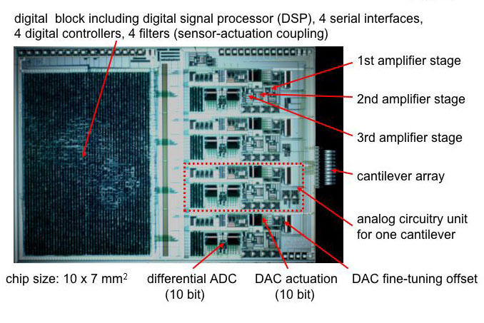
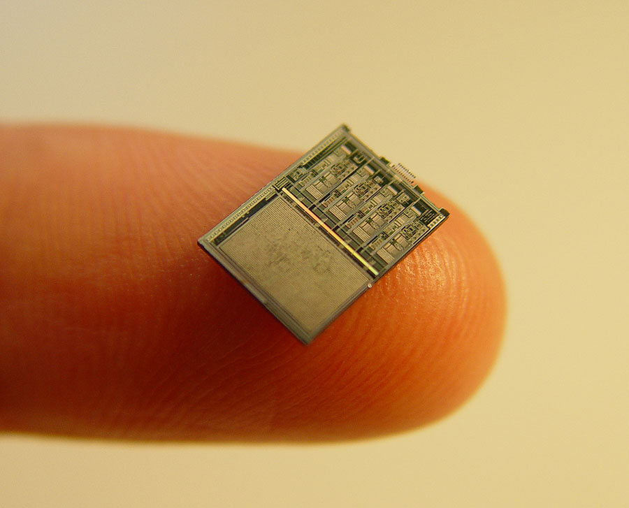
On a CMOS microchip measuring just 7 by 10 millimetres, ETH researchers have managed to realise an entire atomic force microscope. Apart from an array of the micromechanical measuring components–the cantilevers–the miniature apparatus also contains the entire signal processing electronics. The underlying research is described in an article published in the science magazine PNAS (1) By Christoph Meier Progress in the natural sciences always depends, among other things, on the development of new measuring instruments. The development of the raster tunnel microscope, for example, and especially the atomic force microscope in the 1980s, laid the ground for new discoveries without which the boom in nanotechnology would hardly have been possible. With the arrival of the atomic force microscope (AFM) it became possible to measure the forces at the stretching of DNA strands, for instance, or to produce minute transistors lithographically. It is therefore not surprising that such instruments are produced commercially. However, these have some disadvantages: they are quite bulky and, owing to their serial instead of parallel scanning process, have only a low throughput, which means that measurements are time consuming. Cantilevers and the concomitant adjustments of the laser detection cost more time. Professor Andreas Hierlemann and his team at the Physical Electronics Laboratory at ETH Zurich (2) have now succeeded in developing an AFM prototype, which overcomes some of these constraints and which - containing four active cantilevers, as well as the prerequisite electronics - can be placed on a CMOS microchip the size of a fingernail, or to be more exact, 7 by 10 millimetres. CMOS stands for Complementary Metal Oxide Semiconductor, an industrialtandard process in the chip technology. Potent processor Roughly speaking, this chip embodies two main blocks: a digital one, which contains the electronics control, signal processors and a serial interface, and an analogue block, (one for each subunit per cantilever), which contains the filter and amplifier and an analogue-digital converter.
The micromechanical cantilevers are 500 micrometers long and 85 micrometers wide and are manufactured using a micromechanical method within the CMOS process. In order to move the cantilever, the researchers took advantage of the fact that it has two distinct layers, silicon and aluminium. If the temperature of the cantilever is raised over a heating resistor, [?...Heizwiderstand] it begins to bend because the two substances expand at different rates. The bending rate of the cantilever can then be precisely controlled by the heating current. During the scanning of a surface, it now is recorded how strongly a cantilever has to be bent in order for it to exercise constant pressure on the test object. The data thus obtained is then transformed into a topographical display.
|
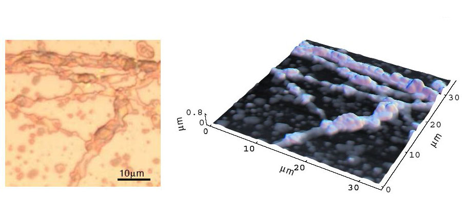
The team of scientists attached four of the ten measuring arms of their microchip to the integrated electronics, enough to test and demonstrate its effectiveness. The electronics serve to amplify the signal, as well as the filtering and offset compensation [?... Offset-Kompensation], and also contains the afore-mentioned analogue-digital converter, a high power digital signal processor and a digital interface. The processor is capable of carrying out up to 16 million arithmetical operations per second, which, according to the ETH researchers represents one of the highest values for CMOS based micro systems. Thanks to this computing power all AFM operations can be executed autonomously, which means that no external signal processing is necessary. Up to 100,000 actuation signals per second can be sent to reposition the cantilever. The computer attached to the microchip therefore only has to assimilate and save the data. When it comes to the spatial resolution, the new instrument detects height differences of less than a single nanometre, or to put it in another way, it can measure differences in force of less than a nanonewton. Using images of etched silicon structures or of nerve-cell endings and force distance curves the ETH research team demonstrates the power of their miniaturised AFMs in a paper published in the science magazine PNAS. Asked about the biggest challenge in the development of AFM, Andreas Hierlemann points to the complexity of the system. It was extremely difficult to integrate digital and analogue electronics and the micromechanical components of the system onto to a chip, although standard procedures already exist for the electronics part. In such a multi-component system, tiny mistakes in a subunit can have fatal consequences for the system as a whole. The ETH scientist sees the application of the miniature AFM, probably the smallest to be developed to date, in situations where a lot of measurements have to be carried out simultaneously. Or where a cantilever cannot easily be replaced, as in astronautics, and where the small dimension and the low weight of the system are deciding advantages.
|
|||||||
|
Footnotes:
You can write a feedback to this article or read the existing comments. | ||||||||